Technology
Myrias Optics
Patent Portfolio Protected Material, Structure and Process
Nanoimprint Lithography (NIL)
No semiconductor fab:
- Rapid, efficient, repeatable and replicative
- Single master yields many stamps, each of which makes thousands of meta-optics
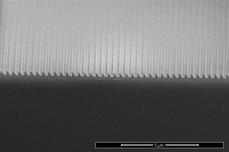
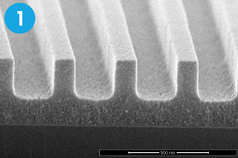
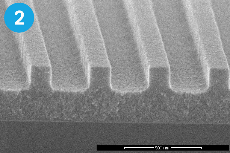
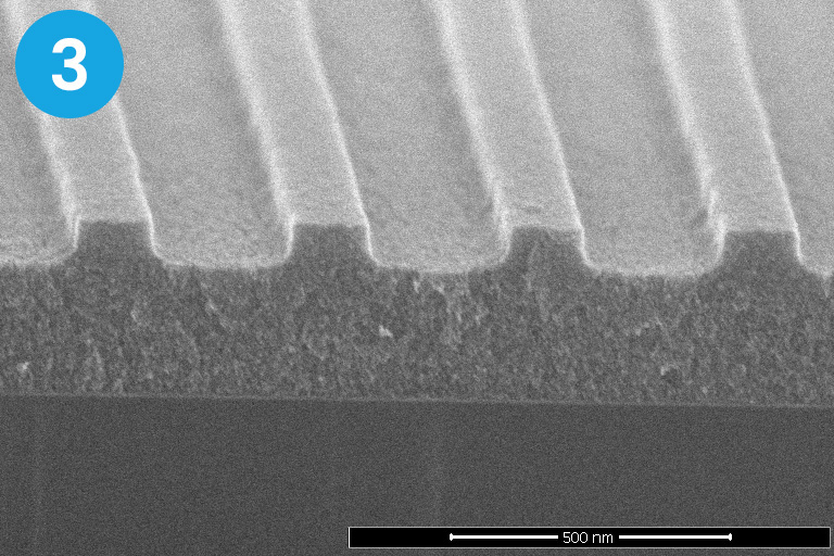
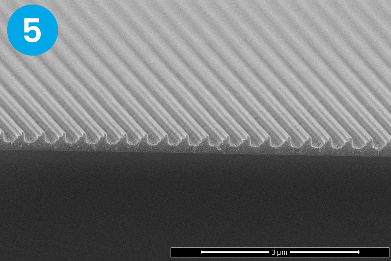
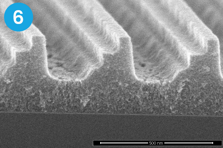
Myrias’ patented platform technology uses direct nanoimprint lithography of nanoparticle composites to provide an all-inorganic, thermally stable, high optical density, low haze and transparent structures with champion optical performance. The material and process combination offers the most promising balance of cost and performance for consumer electronics, defense, AR/VR and next generation machine vision systems.
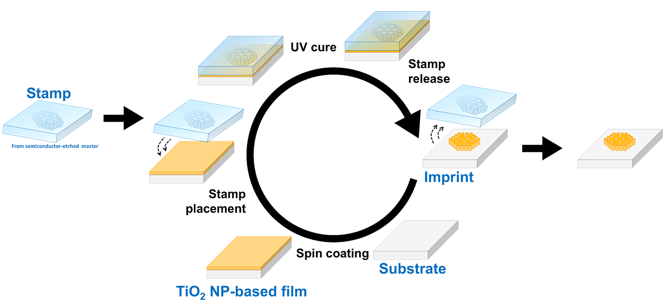
Our Replication Process
The replication process is central to achieving nano-scale resolution over large areas and high volumes. Efficient, non-destructive, copying of the master, first into stamps and then into the nanoparticle composite with low haze, high transparency, high refractive index and exceptional materials stability, yields additively manufactured products with champion performance. In this way, the cost of master fabrication by subtractive semiconductor processing is amortized over tens of thousands of products, which yields unprecedented cost savings relative to optical devices individually fabricated by subtractive processing in a semiconductor foundry.

Low cost
Reduced processing steps and tool requirements.

Thermally and Optically Stable
Careful selection of materials enables use in high energy and extreme environments in addition to extended device lifetimes.

Large Design Scope
The all-inorganic approach enables post processing steps where RI values easily surpasses polymer nanoparticle composites, along with increased optical stability. RI tuning through post processing provides access to new designs and minimizes the impacts of residual layers in imprinted devices.

Highly Transparent
Unlike silicon photonics, Myrias’ technology provides a scalable approach to devices operating at visible wavelengths through the mid infrared.

High Throughput, Large Area
The additive, replicative process provides both more components produced per hour as well as a significantly larger area per device, with the same throughput advantage.


EVG Platform Manufacturing
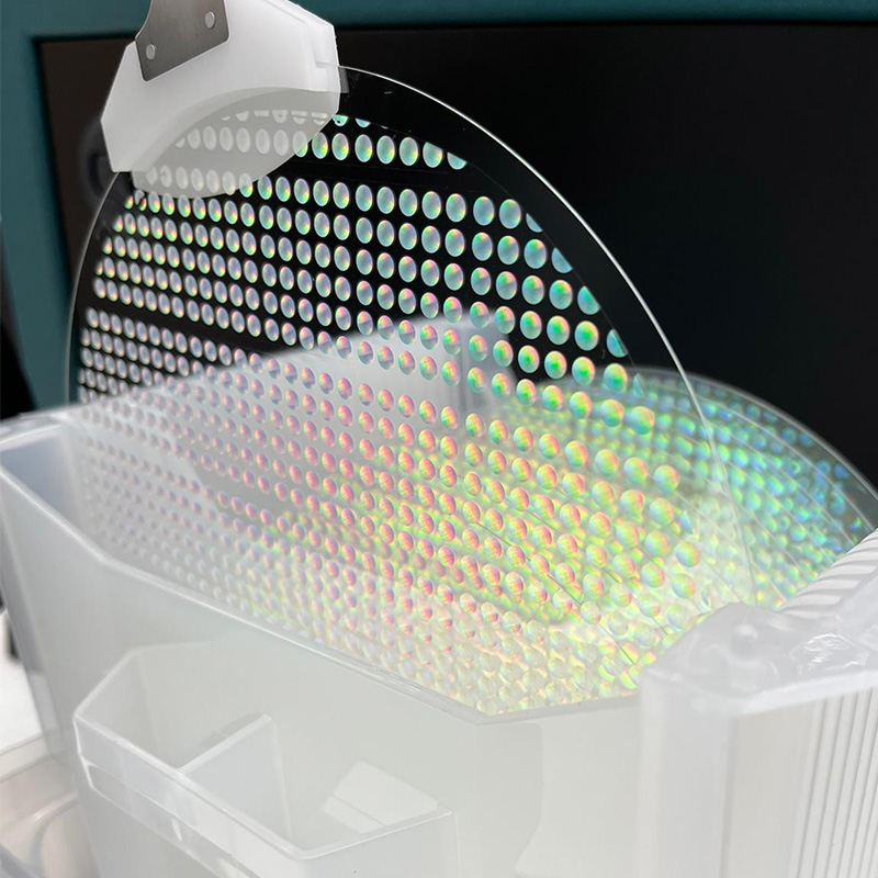
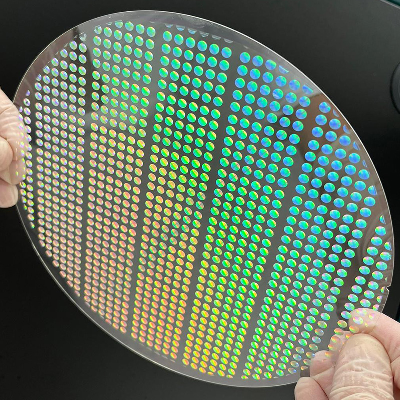
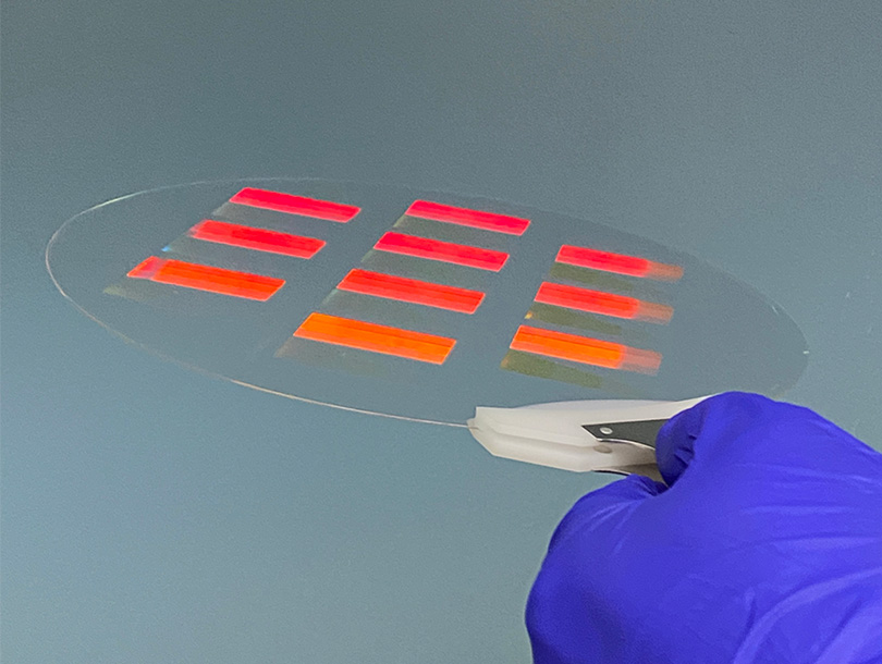
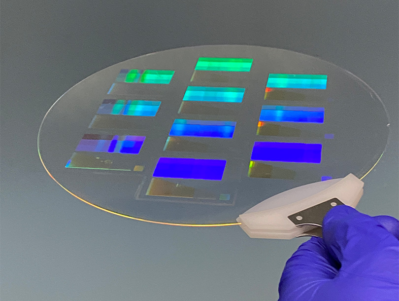
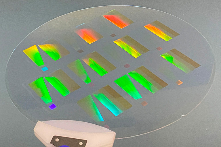
Versatile, efficient manufacturing is critical for securing new markets and high volumes. Myrias has demonstrated full wafer replication on the EVG 7200 platform with high-performance visible wavelength metalenses as well as with AR/VR structures. Along with post-imprint processing options, design constraints can be relaxed and components can be tuned post-fabrication to increase yield, robustness and performance.

Same Structure on Optical Substrate
Real World Solutions
Tool Agnostic Manufacturing
Myrias’ has achieved full wafer manufacturing on multiple tool platforms, paving the way to market with Myrias and your preferred tool partners.
Get in touch!
Wherever you are in the development cycle, Myrias can help move you forward towards higher performance, lower cost and larger scale manufacturing. Myrias welcomes the opportunity to discuss how we can best help you!


